Description
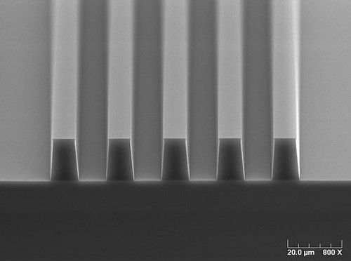
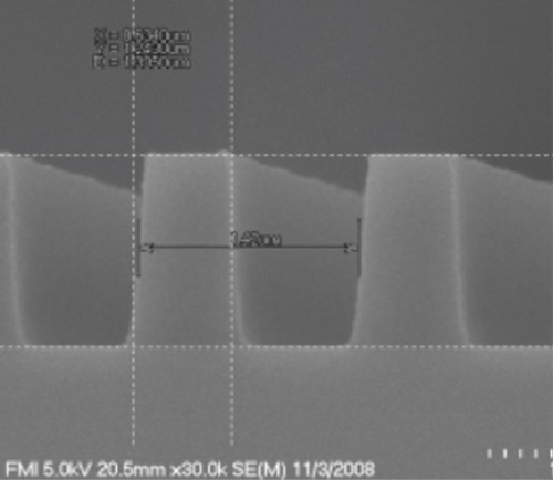
K-PRO™ Advanced Packaging Positive Photoresist is purpose-built for thick-film patterning in packaging and electroplating workflows. Supporting 5–25 µm in a single coat and up to 50 µm via double-coat, K-PRO provides high sensitivity, high throughput, and excellent process latitude on i-line, g-line, and broadband exposure systems. The resist is compatible with plating of copper, pure tin, and nickel and integrates with metal-ion-free or metal-ion-bearing developers to match fab preferences. With no post-exposure bake required, K-PRO streamlines cycle time while maintaining robust feature fidelity across varied wafer topographies in advanced wafer-level packaging, TSVs, bumping, MEMS, and 3D photolithography.
Pricing valid for US, Mexico, and Canada only. Import duties applicable for shipments outside of the US.
Key features
- Tone: Positive
- Exposure bands: i-line, g-line, broadband
- Film thickness: 5 - 25 µm
- Developers: TMAH-based or KOH-based
- PEB: Not required
- Plating compatibility: Copper, pure tin, nickel
- Remover compatibility: NMP or DMSO
- Drop-in Replacement for: AZ P4000 series
Applications
Advanced packaging, TSV, bumping, electroplating molds (Cu pillar, Ni, Sn), and MEMS/3D structures.
Please email info@elexansci.com for MSDS requests.
| Current Resist | KemLab Replacement | Approx. KemLab FT (microns) Range |
| AZ® P4110 | K-PRO 1 | 0.9 – 2.1 |
| AZ® P4110 | K-PRO 2 | 1.3 – 3.6 |
| AZ® P4210 | K-PRO 3 | 2.0 – 5.5 |
| AZ® P4330-RS | K-PRO 5 | 3.0 – 8.0 |
| AZ® P4400 | ||
| AZ® P4620 | K-PRO 7 | 4.1 – 12.0 |
| AZ® P4620 | K-PRO 15 | 7.0 – 25.0 |
| AZ® P4903 |
Cross-Reference Disclaimer: Part numbers are provided for convenience and cross-reference purposes only. These photoresists are manufactured by KemLab and distributed by ELEXAN. AZ® is a registered trademark of MERCK KGAA and our products are not manufactured, sponsored, or endorsed by MERCK KGAA. KemLab and ELEXAN have no affiliation with MERCK KGAA.


